


原子探针断层扫描(APT)
WE KNOW HOW™

Atom Probe Tomography (APT) is a nanoscale materials analysis technique capable of providing three-dimensional (3D) spatial imaging and chemical composition measurements with high sensitivity.
This technique relies on the ionization and subsequent field evaporation of individual atoms/atomic clusters from the sample surface. The sample is prepared in the form of a conical tip with an apex radius of <100 nm. Field evaporation occurs due to a fundamental DC voltage bias (typically between 1–10 kV) and a pulsed voltage (for conductive samples) or a pulsed laser (for semiconductor and insulating samples). Additionally, the sample can be cryogenically cooled to temperatures between 25–80 K to suppress thermal lattice vibrations and improve spatial localization.
2D mapping (device-level): Used to provide information about the device structure and correlate with other techniques.
The field-evaporated ions are collected on a position-sensitive detector (PSD) to accurately determine their x and y positions. The sequence of collected ions is used to derive the z position. Together, x, y, and z provide a spatial image of the sample tip. The time of flight of the ions is also measured and converted into a mass-to-charge ratio for chemical composition analysis. The depth resolution reaches up to 0.3 nm, while the lateral resolution is up to 0.5 nm, though this is limited to metallic samples. For semiconductor and insulating samples, the resolution is lower, typically around 1 nm at best. APT achieves a chemical sensitivity of 10 ppm.
Ideal Applications of Atom Probe Tomography (APT)
-
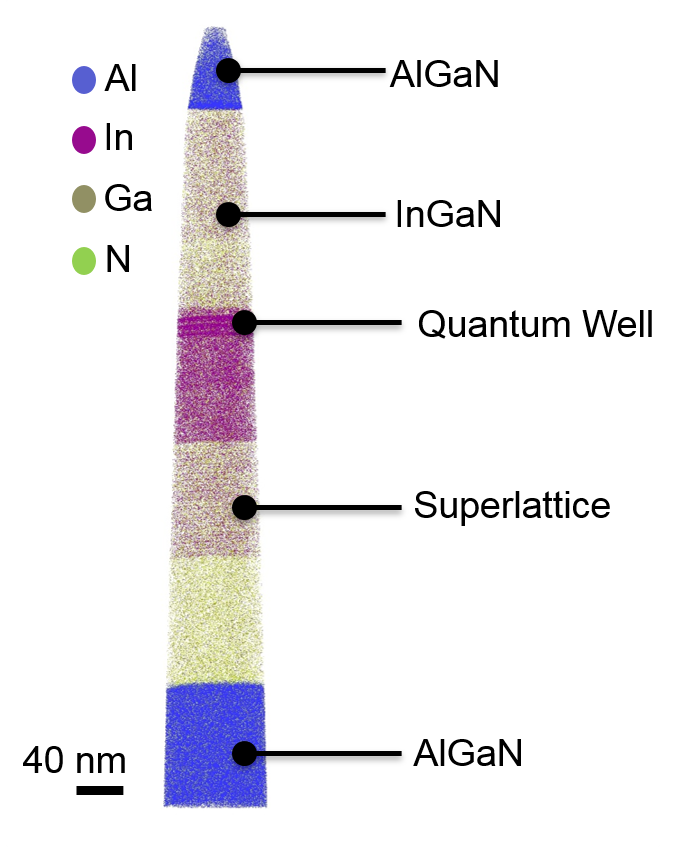
3D structural analysis, e.g., FinFETs, PMOS capping layers, 3D NAND, and curved/irregular grain boundaries in photovoltaics.
-
Nanoscale precipitates and matrix analysis for composition and chemical identification, e.g., metallic alloys (Al 7075, shape-memory alloys, Ti).
-
Light element analysis—Be, B, Li, C, and Al, e.g., lithium-ion batteries.
-
3D dopant mapping for low-concentration dopants in LEDs, FinFETs, 2D NAND memory, and surface coatings of lithium-ion batteries.
Types of Analysis
-
Elemental mapping: Observing the homogeneity/heterogeneity and 2D/3D distribution of chemical species in materials/devices is a key aspect of APT. Typically, 2D maps and 3D reconstructions are used.
-
Compositional variations: APT provides multiple analytical methods, such as depth- or concentration-based line profiles, histograms, and iso-concentration surfaces.
-
Cluster analysis: APT is highly suitable for analyzing nanoscale (1–10 nm) clusters of elements within a matrix. The size and composition of individual clusters, regardless of shape or size, can be characterized. For large cluster populations, further quantitative analysis is possible.
-
Dopant identification and composition: The 3D positions, chemical identity, and number density of dopants (down to ~10 ppm or 5×10¹⁸ atoms/cm³ under optimal conditions) can be determined using APT.
-
Correlative studies: Techniques such as STEM, EBIC, EBSD, electron tomography, and SIMS are routinely combined with APT to enhance 3D data interpretation.
-
Targeted region analysis: Custom combinations of analyses can be performed to investigate specific regions of interest upon request.
Advantages of Atom Probe Tomography (APT)
-
High-resolution dopant mapping in small volumes.
-
Detection and mapping of light elements (e.g., Li, B).
-
Capability to distinguish isotopes.
-
Near-uniform detection probability for all elements (H–U).
-
Cluster analysis of nanoscale precipitates.
-
High mass resolution for identifying diverse elemental species.
Limitations of APT
-
Lengthy sample preparation (4–6 hours).
-
Small analysis volume.
-
Low data acquisition yield due to field instability in some materials.
-
Requires parameter optimization for each material type and structure.
-
Reduced quantitative accuracy for elements with overlapping mass spectra.
-
Heterostructures or complex geometries may suffer from trajectory aberrations, limiting spatial resolution and compositional accuracy.
APT Technical Specifications
-
Analysis type: 3D
-
Material compatibility: Metals, semiconductors, oxides, ceramics.
-
Detectable elements: H–U
-
Detection limit: ~10 ppm (~5×10¹⁸ atoms/cm³)
-
Imaging/mapping: Yes
-
Maximum resolution: 0.5 nm lateral, 0.3 nm depth
-
Analysis area: 50 × 50 nm²
-
Analysis depth: 100–500 nm
-
Ion detection: Positively charged ions
-
Isotope identification: Yes
Contact Us
Submit your inquiry online and we will direct your request to the appropriate technical specialist.
